Wafer Laser Coring, Dicing and Resizing
Overview

Laserod has provided laser wafer coring and resizing services to scores of demanding clients over nearly a generation with precision that can’t be matched with conventional dicing methods.
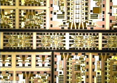
For over thirty years, Laserod has specialized in the coring (resizing), dicing and scribing of silicon wafers for the electronics and other industries. Laser wafer resizing is a more flexible and often less damaging alternative to the conventional mechanical sawing method. Laserod also machines silicon sensors, solar cells, MEMs and other photovoltaic devices by laser dicing or by a two-step scribe-and-break process that converts wafers into “dies” (aka “chips”).
Commonly performed coring jobs are resizing 12″ to 8″ , 8″ to 6″; 6″ to 4″; or 12″, 8″, 6″ or 4″ down to multiple two inch wafers. Practically any kind of downsizing (coring) by laser cutting is possible.
A major advantage of laser wafer dicing over mechanical dicing is the flexibility to create curves, circles and geometries other than a simple array of rectangles. Laser dicing can cut a mixture of various sizes and shapes across a single wafer. The two-step laser scribing process also provides the ability to produce individual dies with minimal debris and low thermal impact.

Laserod’s wafer resizing standard services include:
- Typically silicon, though other materials are acceptable (silicon Carbide, Glass, etc.)
- Resizing/coring from 400mm max diameter to any smaller size and any wafer thickness up to 2mm
- Cutting of flats or notches with tolerances of +/- 0.025mm
- Grinding, typically a rounded or beveled edge
- Video registration through a laser focusing lens, enabling Laserod to register/align to circuitry, fiducial marks or streets and avenues. Registration allows the resized wafer to be precisely aligned to features on the existing wafer, which in turn allows laser cuts to follow the streets and avenues.
Laser Types
Femtosecond
1064nm/532nm/355nm wavelengths
Picosecond
1064nm/532nm/355nm wavelengths
Nanosecond
1064nm/532nm/355nm/266nm wavelengths
Materials
Silicon (Si)
Sipcon Carbide (SiC)
Glass
Sapphire
Ceramic
Bonded Wafers
**Plus many others**
Specs
Wafer Size: Up to 700mm x 700mm
Wafer Thickness: Up to 3mm
Kerf Width: Down to 10ums
Feature Registration: +/-5ums
Notch/Flat Alignment: +/- .1 degrees
Types of Hole Drilling
-

Wafer - Dicing 100um wide street in 500 um thick Silicon
-
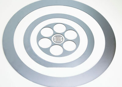
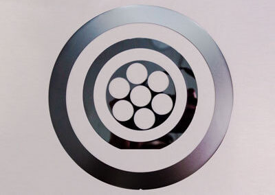
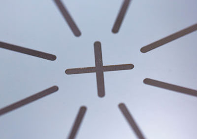
Wafer - Cutting Hole Drilling Custom Design in 500um thick-Silicon 2
-
Wafer - Cutting Hole Drilling Custom design in 500um thick Silicon
-
Wafer - Trenching 150um deep trenches in Silicon (macro-view)
-
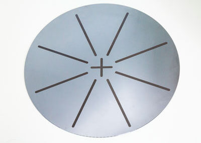
Wafer - Coring Cutting
-
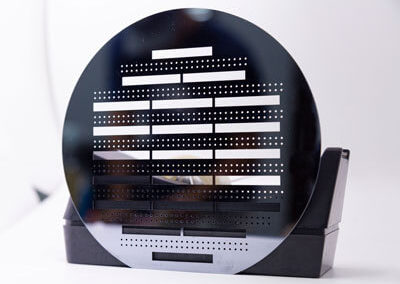
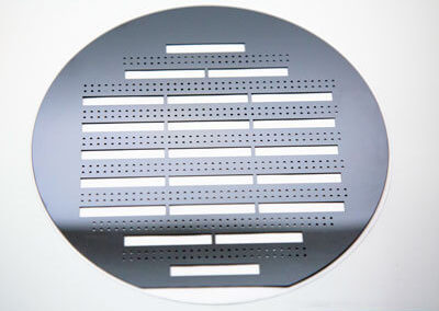
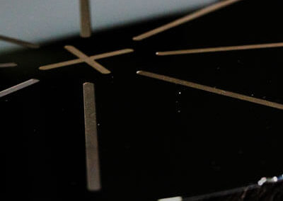
Wafer - Coring Cutting Variety of wafer coring and cutting
-
Wafer - Coring Variety of resized wafers
-
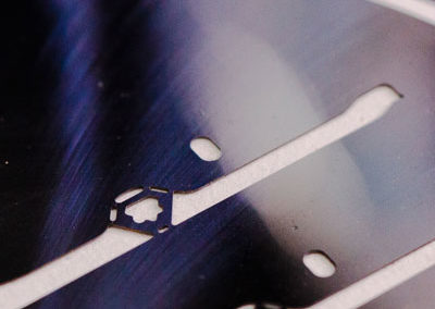
Wafer - Cutting 100um custom feature in 250um thick Silicon
-
Wafer - Trenching 150um deep trench in Silicon (micro-view)
-
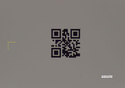
Wafer - Marking Serializing QR Code 395um x 395um
