Our Thin-Film Laser Etching Services
Overview

Laser Thin Film Etching (also called Laser Patterning or Laser Ablation) came into practice first as a means of etching touch panel displays of indium tin oxide (ITO) on a PET sub-surface. Laserod pioneered thin film etching in 1985 when we designed one of the first laser patterning machines for the Fluke Corporation.
Laser etching is a single step, dry etch, non-contact, non-chemical, maskless, ablative process. The conventional method of patterning transparent conductive materials involves a multi-step process using custom masks to selectively exposure photoresist coated substrate that are etched in acid to produce the desired circuit.
Until recent years, the laser etching process was used mainly on R&D applications, as laser patterning could not compete with the high volume production of chemical acid etching. Recent advances in laser and motion technology now allow Laserod to increase our laser ablation rate by a factor of ten, so laser patterning is now found in a number of manufacturing environments from flexible electronics to applications in the energy and medical sectors.
Laser etching offers distinct advantages over other techniques:
- Because it uses no chemicals, laser etching is environmentally green.
- Because the laser is entirely computer controlled, laser etching is easily automated.
- Laser etching setup requires only direct from CAD to substrate programming of a computer, so is more flexible and ideal for quick turnaround time.
- Laser etching can register features down to the micron level.
- Unlike chemical etching, laser etching can be used on a broad variety and types of substrates and materials including glass, plastics and ceramics with ITO, FTO, silver nanowire, carbon nanotubes, chrome, gold and many others.
Some of the many laser patterning projects Laserod has successfully completed include:
- Creating electrode patterns for medical devices
- Ablating turn signal indicators for side mirrors in the automotive industry
- Touch display patterning for the cell phone industry
- Patterning logos
- Creating patterns with ITO, gold, aluminum or copper on glass, quartz or sapphire
- Removing dielectric materials to expose electrodes
- Forming transmissive patterns in optically reflective coatings
- Machining channels in micro fluidic devices
- Marking fiducials and serializing on semiconductor wafers
- Ablating coatings on copper or stainless steel

Our laser etching process removes the invisible and conductive material coating on the display to leave behind a functional circuit, or pattern. The remaining conductive pattern guides the electrical signals to where they are intended. The laser etched patterns are cut from a thin coating of Transparent Conductive Oxide (TCO) on a substrate of glass or plastic film. Examples of TCO are Indium Tin Oxide (ITO), carbon nanotubes, and thin gold coatings. TCO coated glass and plastic are typically used in flat panels, windshields, architectural windows, photovoltaics, and touch screen displays. They are then cut down to 10 micron laser cut widths. For large area removal we simply overlap the ablated 10um spots at high laser repetition rates and at high beam speed to remove large areas of the coatings without damage to the underlying glass or PET substrates.
Laser Types
Femtosecond
1064nm/532nm/355nm wavelengths
Picosecond
1064nm/532nm/355nm wavelengths
Nanosecond
1064nm/532nm/355nm/266nm wavelengths
Coatings
(on glass or plastic)
- ITO
- FTO
- Carbon Nanotubes
- Carbon Nanobuds
- Gold
- Silver
- Chrome
- Silver Nanowire
- Silver Paste
- AZO
**Plus many others**
Specs
Substrate Size: Up to 700mm x 700mm
Line/Gap: Down to 10ums
Feature Registration: +/-5ums
Coating Thickness: Up to 10ums
-

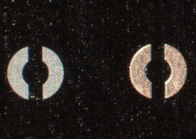
Patterning_Marking--50um feature on Stainless Steel (varying-depths)
-

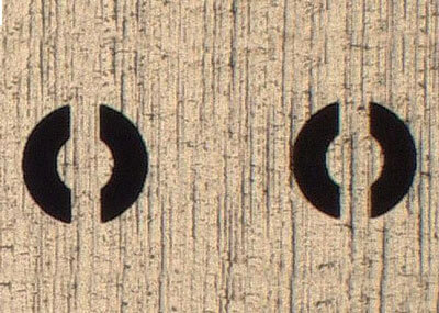
Patterning_Marking--50um feature on Stainless Steel
-
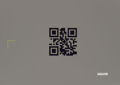
Patterning_Marking--QR Code 395um x 395um
-
Patterning--5um holes in gold coated glass
-
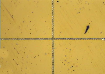
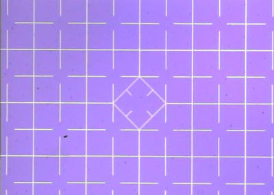
Patterning--15um wide ablation lines on photo resist
-
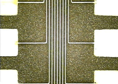
Patterning--20 um wide x 100 um spacing gold removal on glass
-
Patterning--25um wide x 75um pitch ablation of silver paste
-
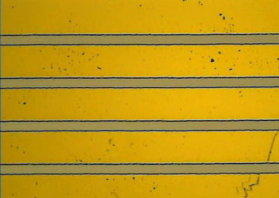
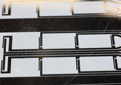
Patterning--30um gap x 100um trace in Silver Paste
-
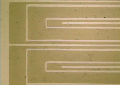
Patterning--30um wide ablation lines in ITO on glass
-
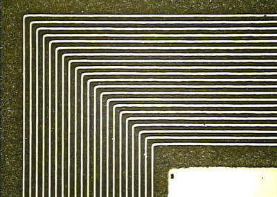
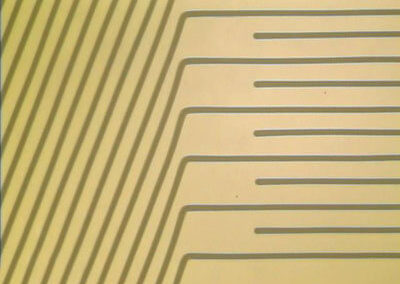
Patterning--40um wide ablation line in ITO
-
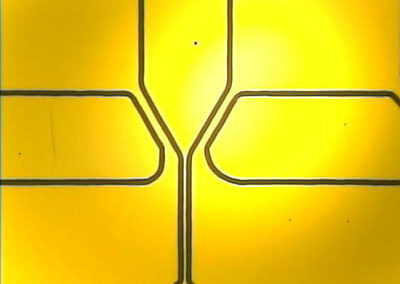
Patterning--50um wide line in thin film gold
-
Patterning--75um gaps on Aluminized PET
Types of Hole Drilling
